- 您现在的位置:买卖IC网 > Sheet目录1999 > IDT2309A-1HPGG (IDT, Integrated Device Technology Inc)IC CLK BUFFER ZD HI DRV 16-TSSOP
6
COMMERCIALANDINDUSTRIALTEMPERATURERANGES
IDT2309A
3.3VZERODELAYCLOCKBUFFER
Output
1.4V
t5
Output
REF
VDD/2
t6
Output
CLKOUT
Device 1
t7
CLKOUT
Device 2
VDD/2
VDD/2
1.4V
t2
t1
1.4V
2V
0.8V
t3
t4
0.8V
3.3V
0V
2V
Output
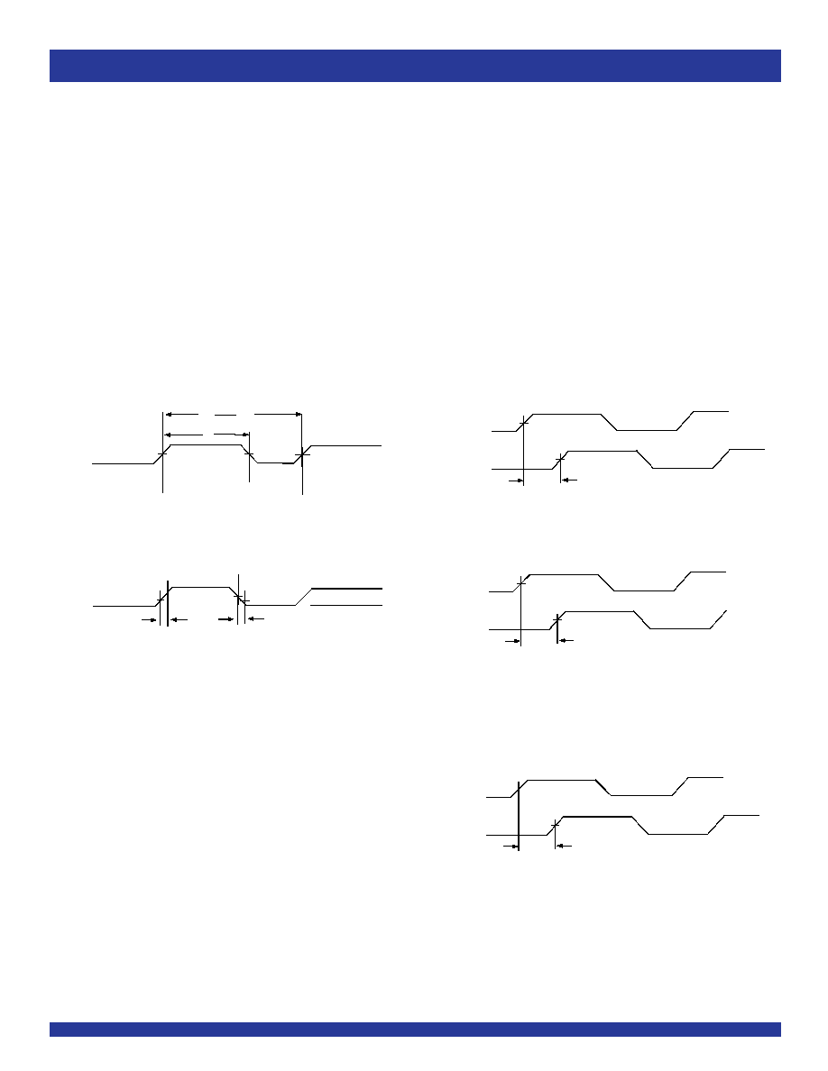
ZERO DELAYAND SKEW CONTROL
All outputs should be uniformly loaded in order to achieve Zero I/O Delay. Since the CLKOUT pin is the internal feedback for the PLL, its relative
loading can affect and adjust the input/output delay. The Output Load Difference diagram illustrates the PLL's relative loading with respect to the other
outputs that can adjust the Input-Output (I/O) Delay.
For designs utilizing zero I/O Delay, all outputs including CLKOUT must be equally loaded. Even if the output is not used, it must have a capacitive
load equal to that on the other outputs in order to obtain true zero I/O Delay. For zero output-to-output skew, all outputs must be loaded equally.
All Outputs Rise/Fall Time
Input to Output Propagation Delay
Device to Device Skew
Output to Output Skew
Duty Cycle Timing
SWITCHING WAVEFORMS
发布紧急采购,3分钟左右您将得到回复。
相关PDF资料
IDT2309B-1HPGGI
IC CLK BUFFER HIGH DRIVE 16TSSOP
IDT23S05-1HDCGI
IC CLK BUFFER PLL HI DRV 8-SOIC
IDT23S05E-1HDCGI8
IC CLK BUFFER PLL HI DRV 8-SOIC
IDT23S08-1HPGI8
IC CLK MULT PLL HI DRV 16-TSSOP
IDT23S08T-1DC
IC CLK MULT PLL ZD 2.5V 16-SOIC
IDT23S09T-1DC8
IC CLK BUFFER ZD 2.5V 16-SOIC
IDT5T929-30NLGI
IC CLOCK GENERATOR PREC 28VFQFPN
IDT5T940-10NLGI
IC CLK GENERATOR PREC 28-VFQFPN
相关代理商/技术参数
IDT2309A-1HPGG8
功能描述:IC CLK BUFFER ZD HI DRV 16-TSSOP RoHS:是 类别:集成电路 (IC) >> 时钟/计时 - 时钟发生器,PLL,频率合成器 系列:- 标准包装:2,000 系列:- 类型:PLL 时钟发生器 PLL:带旁路 输入:LVCMOS,LVPECL 输出:LVCMOS 电路数:1 比率 - 输入:输出:2:11 差分 - 输入:输出:是/无 频率 - 最大:240MHz 除法器/乘法器:是/无 电源电压:3.135 V ~ 3.465 V 工作温度:0°C ~ 70°C 安装类型:表面贴装 封装/外壳:32-LQFP 供应商设备封装:32-TQFP(7x7) 包装:带卷 (TR)
IDT2309A-1HPGGI
功能描述:IC CLK BUFFER ZD HI DRV 16-TSSOP RoHS:是 类别:集成电路 (IC) >> 时钟/计时 - 时钟发生器,PLL,频率合成器 系列:- 标准包装:2,000 系列:- 类型:PLL 时钟发生器 PLL:带旁路 输入:LVCMOS,LVPECL 输出:LVCMOS 电路数:1 比率 - 输入:输出:2:11 差分 - 输入:输出:是/无 频率 - 最大:240MHz 除法器/乘法器:是/无 电源电压:3.135 V ~ 3.465 V 工作温度:0°C ~ 70°C 安装类型:表面贴装 封装/外壳:32-LQFP 供应商设备封装:32-TQFP(7x7) 包装:带卷 (TR)
IDT2309A-1HPGGI8
功能描述:IC CLK BUFFER ZD HI DRV 16-TSSOP RoHS:是 类别:集成电路 (IC) >> 时钟/计时 - 时钟发生器,PLL,频率合成器 系列:- 标准包装:2,000 系列:- 类型:PLL 时钟发生器 PLL:带旁路 输入:LVCMOS,LVPECL 输出:LVCMOS 电路数:1 比率 - 输入:输出:2:11 差分 - 输入:输出:是/无 频率 - 最大:240MHz 除法器/乘法器:是/无 电源电压:3.135 V ~ 3.465 V 工作温度:0°C ~ 70°C 安装类型:表面贴装 封装/外壳:32-LQFP 供应商设备封装:32-TQFP(7x7) 包装:带卷 (TR)
IDT2309A-1HPGI
功能描述:IC CLK BUFFER ZD HI DRV 16-TSSOP RoHS:否 类别:集成电路 (IC) >> 时钟/计时 - 时钟发生器,PLL,频率合成器 系列:- 产品变化通告:Product Discontinuation 04/May/2011 标准包装:96 系列:- 类型:时钟倍频器,零延迟缓冲器 PLL:带旁路 输入:LVTTL 输出:LVTTL 电路数:1 比率 - 输入:输出:1:8 差分 - 输入:输出:无/无 频率 - 最大:133.3MHz 除法器/乘法器:是/无 电源电压:3 V ~ 3.6 V 工作温度:0°C ~ 70°C 安装类型:表面贴装 封装/外壳:16-TSSOP(0.173",4.40mm 宽) 供应商设备封装:16-TSSOP 包装:管件 其它名称:23S08-5HPGG
IDT2309A-1HPGI8
功能描述:IC CLK BUFFER ZD HI DRV 16-TSSOP RoHS:否 类别:集成电路 (IC) >> 时钟/计时 - 时钟发生器,PLL,频率合成器 系列:- 产品变化通告:Product Discontinuation 04/May/2011 标准包装:96 系列:- 类型:时钟倍频器,零延迟缓冲器 PLL:带旁路 输入:LVTTL 输出:LVTTL 电路数:1 比率 - 输入:输出:1:8 差分 - 输入:输出:无/无 频率 - 最大:133.3MHz 除法器/乘法器:是/无 电源电压:3 V ~ 3.6 V 工作温度:0°C ~ 70°C 安装类型:表面贴装 封装/外壳:16-TSSOP(0.173",4.40mm 宽) 供应商设备封装:16-TSSOP 包装:管件 其它名称:23S08-5HPGG
IDT2309A-1PG
制造商:IDT 制造商全称:Integrated Device Technology 功能描述:3.3V ZERO DELAY CLOCK BUFFER
IDT2309A-1PGG
制造商:IDT 制造商全称:Integrated Device Technology 功能描述:3.3V ZERO DELAY CLOCK BUFFER
IDT2309A-1PGGI
制造商:IDT 制造商全称:Integrated Device Technology 功能描述:3.3V ZERO DELAY CLOCK BUFFER